Research Article - European Journal of Applied Engineering and Scientific Research ( 2018) Volume 6, Issue 2
Thallium indium disulfide (TlInS2) single crystals were synthesized by a new local technique called modified Bridgman-Stokbager method. The major results of photoconductivity (PC) for TlInS2 single crystals were obtained within the temperature range of 77 to 300 K, the excitation intensity range of 1000 to 7000 Lux. The applied voltage was from 10 to 70 V and the wavelength range was 400-570 nm. In this manuscript, our results have been elucidated and discussed in different conditions in order to investigate important physical parameters. Dark-and photo-currents have been plotted as a function of the applied bias voltage at room temperature. By applying power law that is “I α f γ “, it was found that the recombination processes in TlInS2 are monomolecular processes. The High photosensitivity of TlInS2 layered single crystals made it possible to study their dc-photoconductivity (dc-PC) spectra in range of the photon energy from 400 to 570 nm. According to the λ1/2 method, the energy gap Eg were computed for the all the temperature range under study as results from the equivalent spectra of the dc-photo conductivity spectra at light intensity 5000 Lux.
TlInS2 single crystals, DC photoconductivity, Energy gap
TlInS2 received scholarly attention because of its electrical and optical properties possibly useful in the fabrication of optoelectronic devices [1,2]. In the last few years, much attention has been devoted to the semiconducting materials of the AIIIBIIICVI group [1,2]. The investigations of physical properties of these chalcogenide semiconductor compounds are necessary for their applications in the modern optoelectronic devices. To the best of our knowledge, no previous work has been reported on a complete study of photoconductivity of TlInS2 single crystals. In the past few years considerable attention has been paid to the investigation of physical properties of layered ternary crystal with chemical formula TIMX2, where (M=Ga, In, X=Se, S, Te). At room temperature, thallium chalcogenides belong to the monoclinic system, and their space group is C2/C. The lattice of these crystals consists of alternating twodimensional layers adjusted parallel to the (001) plane [1]. The TlInS2 single crystal is a semiconductor with an indirect band gap of about 2.28 eV at room temperature [2]. Deiseroth and Walther [3] synthesized ternary solids and thoroughly investigated the crystal structure and some common characteristics. The effect of electron radiation on dielectric properties of TlInS2 single crystals has been reported by Yossef and Natig [4]. Yossef and Natig [5] also investigated the fundamental absorption edge for monoclinic TlInS2 crystals in the temperature range of 4.2 to 300 K. Kalkan [6] studied the structure and photo electronic properties of theTlInS2 crystal. They concluded that TlInS2 sample has a long-term superstructure which appears to come from a tetragonal basic structure with a=b=7.64 Å and c=19.5 Å. This may be due to the arrangement of the large number of planar faults parallel to the (001)teeter-plane. Two energy levels restricted at 0.028 and 0.50 eV above the valence band edge, eV, with capture coefficients of the order of magnitude 10-13 and 10-15 cm-3s-1 at 300 K were detected. Their concentrations were of the arrangement of the magnitude of the concentration of atoms in solid matter. Ozdermir et al. [7] studied the effect of illumination and temperature on both photocurrent and thermally stimulated current spectra of TlInS2 single crystal. Aydinli et al. [8] showed the photoluminescence (PL) spectra of TlInS2 crystal in the range of 500-860 nm. Badr et al. [9] recently investigated the photoelectric properties of TlInS2 layered single crystal, where the transmittance and reflectance spectra of TlInS2 crystals (1.96-2.46 eV) were measured in the temperature range of 77-300 K. The optical properties of TlInS2 layered single crystals have been studied by El-Nahass et al. [10] using spectrophotometer measurements of transmittance and reflectance in the wavelength range of 200-2500 nm. Nagat et al. [11] investigated the switching phenomenon in single crystal TlInS2 which reveals that it may be a utilitarian material for the fabrication of switching devices. Isik et al. [12] studied the trap centers and distributions in TlInS2 within the temperature range of 100-300 K by using the thermally stimulated current technique. Shim [13] the in-commensurate material, TlInS2, with layer structure was carefully considered by light figure spectroscopy techniques in spectral range 400-700 nm in temperature interval 80-350 K. The study of temperature dependence of the optical second-harmonic generation in TlInS2 crystals in the vicinity of phase transitions has been carried out [14]. Isik et al. [15] measured two-photon absorption (TPA) coefficients for layered chalcogenide crystals TlGaSe2, TlInS2, TIGaS2 and GaSe. The infrared transmittance and Raman scattering spectra in TlGaS2, TlInS2 and TlGaSe2 layered single crystals grown by the Bridgman method was observed by Ashraf et al. [16] in the frequency range of 400-1500 and 10-400 cm, respectively. Ashraf et al. [16] studied the infrared transmittance and Raman scattering spectra in TlGaS2, TlInS2 and TlGaSe2 layered single crystals grown by the Bridgman method in the frequency range of 400-1500 and 10-400 cm, respectively. The III-VI group binary semiconducting compounds have interesting physical properties and they have widely been used in many electronic devices. Due to these interesting properties, these compounds are attracting many authors for further study. This paper reports the preparation of TlInS2 single crystals by a new local technique known as modified Bridgman- Stokbager method and a thorough study of the photoconductivity (PC) of these TlInS2 single crystals.
TlInS2 single crystal was grown up by the Bridgman technique [17]. TlInS2 was prepared from high-purity (99.999%) thallium, indium and sulfur as initial components. The compositions of all the required components are 13.6256 g of thallium (43.221%), 11.4868 g of indium (36.437%) and 6.413 g of sulfur (20.342%). The modifications studied by fusing the constituent elements into an evacuated (10-6 Torr) silica tube of 1.5 cm diameter and 20 cm in length. The crystal structure of the grown compound was investigated using x-ray diffraction method at room temperature.
The sample, which was used in the PC measurements, was prepared in a rectangular shape with the required dimensions and high-quality polishing surface. The specimen dimension was measured by traveling microscope of high sensitivity (0.0734 × 0.0413 × 0.009 cm). Such a specimen used in the measurements of our compound (TlInS2 crystals) was prepared by cutting crystal along the cleavage planes; the resulting surfaces were mirror-like. It was polished by using various degrees of polishing disks with which the specimen dimensions were controlled to obtain the desired dimensions for each property (PC). Finally, the resulting specimens have highly polished flat surfaces that were cleaned for their uses. Then the sample was fitted onto the cold finger inside a cryostat (Oxford DNI 704- type), which can be evacuated up to a pressure of about 10-4 Torr. Since the aim of present work is mainly to describe the temperature dependence of the various physical properties of TlInS2 crystals; therefore a stabilization system is needed. The specimen under study was mounted on the cold finger of the holder inside an Oxford crystal of type DNV2 (temperature range of 77-300 K). This crystal was evacuated up to a pressure of about 10-4 Torr as it is important to prevent water vapor condensation at low temperatures and also to protect sample oxidation at high temperatures. In this experiment, a beam of monochromatic light is incident at the right angle to the crystal surface plane. The applied voltage was adjusted to the desired values by using a suitable voltage divider and its values were recorded by a sensitive voltmeter. The current values were measured by using electrometer. The white light was supplied from a tungsten lamp of about 1000 W. An optical system composed of two convex lenses was used to obtain a focused light to be incident on the sample. The light intensity could be controlled by a suitable transformer connected to the tungsten lamp. We used a digital lux meter to measure the intensity of incident light. The monochromatic beam of light was obtained by using a monochromatic.
Structural properties of TlInS2 single crystals
The crystal structure of grown crystal was identified using X-ray diffraction (XRD) analysis at room temperature. This has been done by using a modern automated and computerized diffract meter with CuKα radiation (λ=1.54 Å), operated at a voltage and current of 40 KV and 30 mA and the scanning speed of 0.020/s. Our result of the XRD patterns for TlInS2 crystal in the powder form is shown in Figure 1. The interplanar distance (d) for each peak was calculated using the well-known Bragg’s law nλ=2d sin(θ) and the relative intensities (I/Io) were also determined.
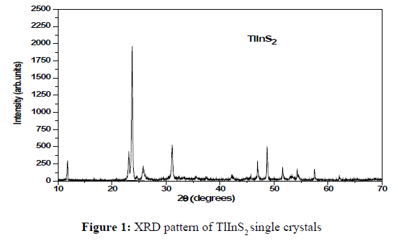
Figure 1: XRD pattern of TlInS2 single crystals.
Diffraction patterns of our crystal were compared with the standard cards (N.I.S.T.) and previous result. So the nature of the obtained crystals has been asserted by comparing the values of the interplanar distance (d) computed from the peaks and those from the previous results [18]. One may easily observe that the crystals have a high degree of crystalline evidence and the preparation technique is impartially reliable and acceptable. The above comparisons showed that, the resulting TlInS2 compound has monoclinic crystal structure with lattice parameters: a=0.3763, b=0.3964, c=0.7726 nm and β=97.310. These results may differ with some of the results of the crystal structure, which has been presented in previous works [6,19-21]. These divergences may probably be related to different modifications of the crystals studied [18].
Dc-photoconductivity of TlInS2 single crystals
The dependence of the dark current and photocurrent measured on the applied voltage for TlInS2 single crystals are clarified in Figure 2. This figure showed that the dark current as well as the photocurrent linearly increases with the increase in voltage.

Figure 2: Dark current and photocurrent as a function of voltage at different levels of illumination for TlInS2 single crystals.
The photosensitivity calculated for TlInS2 single crystals for different levels of illumination.

Where represent photoconductivity and dark conductivity, respectively.
The photocurrent was drawn up as a function of the light intensity as shown in Figure 3. One may observe from this figure that the photocurrent linearly increases with the intensity of light, which is due to the generation of large numbers of free charge carriers. So the relation between the photocurrent and light intensity obeys the power law [22].

Figure 3: The photocurrent as a function of the light intensity for TlInS2 single crystals.

Where Iph is the photocurrent, f is the average of optical excitation, which this rate of optical excitation is proportional to the light intensity for normal light intensity, and γ is a constant whose value determines the type of recombination process. For γ=0.5, the recombination process is bimolecular, but for γ=1 the recombination process is monomolecular (linear). If the value of γ lies between 0.5 and 1 (sublinear), it suggests that there is a continuous distribution of impurity states [23]. In our study of TlInS2 single crystal, it is found that the value of γ equal to 1.05 shows that the combination process in TlInS2 single crystals is a monomolecular process.
The high photosensitivity of TlInS2 single crystals made it could be to study dc-PC spectra in a wide range of the photo energy. The spectral distributions of the photocurrent for TlInS2 single crystal were studied in the wavelength range of 400 nm to 570 nm at different values of temperature, applied voltage and light intensity. The photocurrent was obtained by subtracting the value in the darkness from that of under illumination. Figures 4-7, represent the spectral distribution of dc-PC for TlInS2 single crystal in the different interval of temperature ranges from 77 up to 300 K, 77 to150 K, 175 to 225 K and 250 to 300 K respectively. In this experiment a voltage of 50 V was applied to the sample under investigation with a light intensity of 5000 Lux, these were used for the excitation process. Figure 4 shows the variation of dc-PC spectra in the temperature range of 77 to 300 K, in which the response of the photocurrent is not clear for low temperatures because of its dependence on temperature. The spectral distribution of the photocurrent was separated into three ranges that are 77 to 150 K, 175 to 225 K and 250 to 300 K, and was plotted separately, as shown in the Figures 5-7, respectively. The dc-PC spectra have one photo-peak in the temperature range of 77 to 300 K which is connected with direct. Band-Band transition, for 77 K, the photo-peak was found at 2.817 eV, which moves slightly toward low photo energy side with increasing temperature and the photo-peak was observed at 2.666 eV when the temperature reach at 300 K. These figures shows that the highest value of the photocurrent (photo-peak) increases by increasing the temperature from 77 to 150 K and also increases with increasing temperature from 250 to300 K. But in the range of 175 to 225 K the photocurrent decreases with increasing temperature.

Figure 4: The spectral distribution of the dc-PC for TlInS2 single crystal in the temperature range of 77 to 300 K.

Figure 5: The spectral distribution of the dc-Pc for TlInS2 single crystal in the temperature range of 250 to 300 K.

Figure 6: The spectral distribution of the dc-Pc for TlInS2 single crystal in the temperature range of 175 to 225 K.

Figure 7:The spectral distribution of the dc-Pc for TlInS2 single crystal in the temperature range of 77 to 150 K.
This behavior became clear when we studied the dependence of photocurrent on the temperature at the highest value of photon energy (3.1 eV) in the extent of the study, as shown in Figure 8. The reason behind the increase of the photocurrent with temperature (in the temperature range of 77 K-175 K and 225K -300 K), may be due to the increase of free charge carriers. But the decrease of photocurrent in the temperature range of 175 K-225 K is mainly due to the phase transition in the sample, as it has been reported by the Ozdemir et al. [24] that the phase of the sample in the temperature range of 175-225 K changes from para- to ferro-electric phase. This transformation process may be a cause for reduced photocurrent in the temperature range of 175-250 K due to the change of the strain energy for this sample during the phase transformation process in this interval temperature [25].

Figure 8:The variation of photocurrent with temperature forTlInS2 single crystal.
Mathematically, the spectral sensitivity can be calculated by the relation:

Where B is a constant, E is the energy at any wavelength and Eo is the energy at the threshold wavelength. This curve has a smooth reaction at short wavelength and an exponential fall with energy at long wavelength. It is supposed that the changing sensitivity results due to the apportionment of the energy levels. These energy levels originate photoelectrons, which transport from it. The existence of such distribution centers was confirmed by Busch [25] and Rose [26]. If we suppose that N(E)dE illustrates the number of energy levels per unit volume lying between E and E+dE. Then, as the material is irradiated by a given quantum energy Eλ, the amount of absorption and therefore the sensitivity will be proportionate to the total number of centers of energy lower than Eλ [27].
Where G is a constant, substituting Equation 3 in Equation 6, we obtain:

From this expression and using the distribution of energy levels, we can calculate the number of electrons present in the conduction band due to thermal excitation from level E as follows:

Where C is a constant
This relation is analogous to the relation obtained for the Hall Effect using the simple theory of electrons, which is excited into the conduction band from one definite energy level [28]:
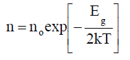
Where Eg is the width of the forbidden band gap for intrinsic conductivity. Hence, by comparing Equation (8) and Equation 9, we get Eg=Eo. Therefore the sensitivity S can be described by the following relation:

It should be mentioned here that the activation energy is specified from the spectral curve at a point where the sensitivity has tumbledown to half of its value, that is:

Therefore, at λ1/2, we can determine the forbidden band gap width (Eg) as:

According to the λ1/2 method, the value of energy gap Eg can be studied for all the temperature range under study as results from the corresponding dc-PC spectra at the light intensity of 5000 Lux. By representing the estimated values of the band gap against the congruent temperatures, it was found that the energy gap of TlInS2 single crystal decreases as temperature increases. It’s clear from the Figure 9 that the value of Eg at room temperature is 2.316 eV, however, at 77 K, it was found to be 2.402 eV.
The energy gap for TlInS2 crystal decreases as temperature increases, and can be governed by the relation [29]:

Where the first term depends on the lattice expansion and the second term depends on the electron-phonon interactions. Our results suggest that the role of electron-phonon interaction is larger than that of the lattice expansion.
Such behaviors typical for the crystals having layered structure [29] and its temperature coefficient (dEg /dT) was calculated from the straight-line portion of Figure 9 that results to the value of -3.65108 × 10⁻⁴ eV/K.

Figure 9:The variation of the energy gap as a function in the temperature at light intensity 5000 Lux.
The dependence of Eg on temperature is governed by the following empirical expression:

Where Eg (0) is the energy gap at 0K, and its observed value is 2.411 eV, whereas α, β are fitting parameters characteristic of a given material, since β which is supposed to be related to the Debye temperature. Both α and β were evaluated and found to be about 5.472 × 10⁻⁴ and 249.541, respectively.
The spectral distributions of the dc-PC at different bias voltages and light intensities for TlInS2 single crystal in the wavelength range from 400 to 570 nm are shown in Figures 9 and 10. At different values of the applied voltage (from 10 to70 V) the dc-Pc of our compound were measured at constant temperature of 300 K and light intensity of 5000 Lux. The spectral distribution at different light intensities (from 1000 to 7000 Lux) was ascertained with firm value of temperature and applied voltage (300 K and 50 V). The format of the spectral distribution characteristics was especially independent of both the light intensity and the applied bias voltage. It was found that the photocurrent shifts toward its higher values as light intensity and applied bias voltage increase. This suggests that the number of excited carrier’s increases with the intensity of light, as a result the photocurrent also increases. It is spotted that the photocurrent transfers on behalf of its higher values as light intensity or applied bias voltage increases shown in Figures 10 and 11. The relation between the carrier velocity ?, the carrier mobility μ and the electric field E can be simply written in the form ?=μ E which shows that ? is proportional to the applied voltage V ( as E is proportional to V).

Figure 10:The spectral distribution of the dc-PC for TlInS2 single crystal at different values of the applied voltage.

Figure 11:The spectral distribution of the dc-PC for TlInS2 single crystal at different values of the light intensity.
So the light intensity generates the carriers to be drifted by increasing the applied voltage driving to an increase in the carrier velocity.
The aim of our present work is to prepare TlInS2 single crystals by anew local technique modified Bridgman-Stokbager method, and study of photoconductivity (PC) for TlInS2 single crystals. Results are obtained in the temperature range from 77 to 300 K, excitation intensity range from 1000 to7000 Lux, applied voltage range from 10 to 70 V and in the 400-570 nm wavelength range. Both the ac-photoconductivity (ac-PC) and the spectral distribution of the photocurrent are studied in different values of light intensity, applied voltage and temperature.
Dependencies of carrier lifetime on light intensity, applied voltage and temperature are also investigated as a result of the ac-PC measurements. By using the results of the dc-photoconductivity (dc-PC) measurements, the temperature dependence of the energy gap width is described.
“The author(s) declare(s) that there is no conflict of interest regarding the publication of this paper”.